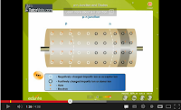
The p-n junction

- We can produce a single crystal with a p-type semiconductor on one side and n-type on the other side as shown in the figure above.
- The border where the p-type and the n-type region meet is called the p-n junction.
Depletion Layer and Junction Voltage
- At the p-n junction, electrons from the n-type semiconductor will be attracted to the holes in the p-type semiconductor.
- As a result, the holes and the electrons at the p-n junction disappear, forming a layer called “depletion layer”.
- At the same time, the p-type semiconductor becomes more negative whereas the n-type semiconductor becomes more positive.
- This will result in a potential difference across the p-n junction. This potential difference is called the junction voltage (or the barrier voltage).
- The junction voltage will prevent the charge carrier from flowing across the depletion layer.
Recommended Videos

Formation and Properties of Junction Diode – Physics
This is a physics video for Grade 11-12 students about p-n junction diode, its properties, characteristics and uses. The combination of p-type and n-type semiconductors results in a junction. When a p-type semiconductor is joined with n-type semiconductor, the resultant junction formed is called a p-n junction diode.